-PVD 물리 증착법 : 시간이 적게 드는 특징이 있다. (ex : 열증착, E-beam 증착법)
-CVD 화학 증착법 : 오래 걸리지만 박막을 표면에 고르게 증착시킬 수 있다.
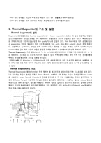
1. Thermal Evaporator의 구조 및 설명
Thermal Evaporator의 설명
Evaporation의 방법으로는 thermal evaporation과 e-beam evaporation 그리고 이 둘을 조합하는 방법
Vacuum)에서 이루어진다. ingot의 양에 증착되는 film의 양을 control 할 수 있으며 열전자를 사용하기 때문에 융점이 높은 물질도 쉽게 증착 할 수 있는 장점이 있다.
electron beam
To Vacuum Pumps
vapor stream
substrate holder
Three Ingot Feeders
Four Independent
ion Sources
To Vacuum Pumps
electron gun
그림2. E-beam장치의
Vacuum Pumps
vapor stream
substrate holder
Three Ingot Feeders
Four Independent
ion Sources
To Vacuum Pumps
electron gun
그림2. E-beam장치의 구조도
② Thermal Evaporator
각종 금속(Au, Al, Ti, Cr, In, Ni)과 유전체(SiO2)의 박 막을 기판 위에 증착할 수 있는 장비이다. 진공도는 Torr까지 얻을 수 있다. 박막 증착시에는 박막
1. Cleaning
- For elimination particle
2. Deposition
- Formation some material layer on the substrate
3. Photolithography
- Formation some pattern
4. Etching
- Elimination substrate or PR layer
Material to be evaporated is heated to
increase vapor pressure
In a reasonably high vacuum, material
atoms fly to a target and stick onto the
surface
Source materi
Vacuum and freeze drying processes are used for products with delicate flavours and textures like coffee granules, eggs, prawns and vegetables. The process involves freezing, and evaporating the ice away, under reduced pressure. It is an expensive process but gives a produce which is high in flavour and palatability. Milk may be dried on rollers or by spraying concentrated milk into hot air chamb
투과전자현미경은 주로 시료의 내부구조나 단면을 관찰하는데 쓰이고 있다. 원리는 광학현미경과 비슷하다. 전자현미경에서의 광원은 높은 진공 상태(1x10⁻⁴ 이상)에서 고속으로 가속되는 전자선으로 이 전자선이 표본을 투과하여 형광판이나 사진필름에 초점을 맞추어 투사된다. 이 전자의 파장은 가
The threshold voltage of a MOSFET is usually defined as the gate voltage where an inversion layer forms at the interface between the insulating layer (oxide) and the substrate (body) of the transistor. The purpose of the inversion layer's forming is to allow the flow of electrons through the gate-source junction. The voltage of oxide is given by
V_OX= 1/C_OX 2√(qN_A ε_Si V_0 )
SiO_2 V_O
② Thermal Evaporator
각종 금속(Au, Al, Ti, Cr, In, Ni)과 유전체(SiO2)의 박 막을 기판 위에 증착할 수 있는 장비이다. 진공도는 Torr까지 얻을 수 있다. 박막 증착시에는 박막 두께 측정 센서를 통해 박막의 두께를 확인하며 공정을 진행할 수 있다. 박막은 보통 0.5 Aring/sec ~ 1.0 Aring/sec의 증착 속도로 증착을 하
[3] Thin Film Deposition
초집적 반도체를 구성하는 소자들은 그 특성상 그 크기가 매우 얇아(작고) 미세한 조직을 가진다. 그리고 이것은 박막 증착(TFD = Thin Film Deposition) 공정을 통해 제작된다. 박막 증착이란 이름 그대로 표면에 얇은 막을 씌우는 기술을 뜻하는데 이 공정을 통해 기판(substrate)이나 이전에
2.3 C-V graph
The measured MOS capacitance (called gate capacitance) varies with the applied gate voltage.
① Measurement of C-V characteristics
-Apply any DC bias, and superimpose a small (15 mV) ac signal
-Generally measured at 1 MHz (high frequency) or at variable frequencies between 1KHz to 1 MHz
-The dc bias VG is slowly varied to get quasi-continuous C-V characteristics
② C-V chara